You are using an out of date browser. It may not display this or other websites correctly.
You should upgrade or use an alternative browser.
You should upgrade or use an alternative browser.
Anyone here a systems engineer?
- Thread starter naisho
- Start date
The Highlander
New Member
- Joined
- Mar 16, 2007
- Messages
- 8,235
- Reaction score
- 1
I know my friend who process engineer at Intel
VacationGuy234
Active Member
- Joined
- Aug 21, 2011
- Messages
- 4,030
- Reaction score
- 4
I've a question I need to ask, it probably isn't too bad if you know about small scale consumer computer electronics and software integration.
What is the actual question? Are you trying to solve something?
- Joined
- Jan 25, 2010
- Messages
- 2,635
- Reaction score
- 83
I am...or let say...we are....
Here's the link: http://www.keywcorp.com/solutions_003.html
This is our company I work for....
Here's the link: http://www.keywcorp.com/solutions_003.html
This is our company I work for....
naisho
Forum Disorders M.D.,Ph.D
- Joined
- Nov 6, 2006
- Messages
- 6,432
- Reaction score
- 12
Alright, cool, maybe you can help me figure this out. This wasn't something I can google up and find an answer, I'm not seasoned in software engineering and integration.
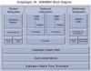
I was looking for block diagrams for the Qualcomm Snapdragon S2 chipset to reference for how the camera is integrated. Unfortunately, Qualcomm never released much information about their Snapdragon generation 2 chipsets. I only found schematics for the next generation S4 and the detail is very limited, see below.

So I can't figure out who is responsible for the camera integraiton. I'm trying to see who is responsible for camera chipset driver development in the phones we have today. Specifically, in the case of the S2 chipset, I'm clueless whether it's between Qualcomm is responsible for the drivers or it is between a proprietary OEM supplier like HTC, or would it be Adreno (Qualcomm's graphics/HW video acceleration division).
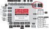
However, I did find out that Texas Instruments released schematics for their TI OMAP 44xx series, namely the same chipset used in the Samsung Galaxy Nexus / Google Galaxy Nexus (OMAP 4460). I circled the part I noticed responsible for camera integration on the SoC.

As I saw from the block diagram, The MIPI alliance seems like it made the camera chipset/instructions, but obviously it's all integrated into part of the OMAP44xx SoC, so that would point to TI being responsible for development of the camera integration with chipset programming and drivers, not Samsung (for the Galaxy Nexus), and probably not PowerVR (for the PowerVR SGX540 GPU development). That is how I seem to understand this.
Can you tell me if I'm on the right track? I'm having a bit of a hard time figuring this all out because I'm not a systems engineer, this is a bit out of my scope to understand 100% how everything works.
I was looking for block diagrams for the Qualcomm Snapdragon S2 chipset to reference for how the camera is integrated. Unfortunately, Qualcomm never released much information about their Snapdragon generation 2 chipsets. I only found schematics for the next generation S4 and the detail is very limited, see below.
So I can't figure out who is responsible for the camera integraiton. I'm trying to see who is responsible for camera chipset driver development in the phones we have today. Specifically, in the case of the S2 chipset, I'm clueless whether it's between Qualcomm is responsible for the drivers or it is between a proprietary OEM supplier like HTC, or would it be Adreno (Qualcomm's graphics/HW video acceleration division).
However, I did find out that Texas Instruments released schematics for their TI OMAP 44xx series, namely the same chipset used in the Samsung Galaxy Nexus / Google Galaxy Nexus (OMAP 4460). I circled the part I noticed responsible for camera integration on the SoC.
As I saw from the block diagram, The MIPI alliance seems like it made the camera chipset/instructions, but obviously it's all integrated into part of the OMAP44xx SoC, so that would point to TI being responsible for development of the camera integration with chipset programming and drivers, not Samsung (for the Galaxy Nexus), and probably not PowerVR (for the PowerVR SGX540 GPU development). That is how I seem to understand this.
Can you tell me if I'm on the right track? I'm having a bit of a hard time figuring this all out because I'm not a systems engineer, this is a bit out of my scope to understand 100% how everything works.
Attachments
- Joined
- Jan 25, 2010
- Messages
- 2,635
- Reaction score
- 83
Alright, cool, maybe you can help me figure this out. This wasn't something I can google up and find an answer, I'm not seasoned in software engineering and integration.
I was looking for block diagrams for the Qualcomm Snapdragon S2 chipset to reference for how the camera is integrated. Unfortunately, Qualcomm never released much information about their Snapdragon generation 2 chipsets. I only found schematics for the next generation S4 and the detail is very limited, see below.
So I can't figure out who is responsible for the camera integraiton. I'm trying to see who is responsible for camera chipset driver development in the phones we have today. Specifically, in the case of the S2 chipset, I'm clueless whether it's between Qualcomm is responsible for the drivers or it is between a proprietary OEM supplier like HTC, or would it be Adreno (Qualcomm's graphics/HW video acceleration division).
However, I did find out that Texas Instruments released schematics for their TI OMAP 44xx series, namely the same chipset used in the Samsung Galaxy Nexus / Google Galaxy Nexus (OMAP 4460). I circled the part I noticed responsible for camera integration on the SoC.
As I saw from the block diagram, The MIPI alliance seems like it made the camera chipset/instructions, but obviously it's all integrated into part of the OMAP44xx SoC, so that would point to TI being responsible for development of the camera integration with chipset programming and drivers, not Samsung (for the Galaxy Nexus), and probably not PowerVR (for the PowerVR SGX540 GPU development). That is how I seem to understand this.
Can you tell me if I'm on the right track? I'm having a bit of a hard time figuring this all out because I'm not a systems engineer, this is a bit out of my scope to understand 100% how everything works.
Aaaah..I'll pass it on to Dave (expert on camera enginneer).. He will be glad to answer it... (if he's in today due to holiday)
Zeroblazer21
Member
- Joined
- Apr 10, 2008
- Messages
- 445
- Reaction score
- 1
isnt this is a design of android processor for newer gen of android (dual core)?
if you're seeking for a hint, advice, etc i suggest you go to overclocking.net they know deep shits about engineer. unlike me. i'm more like a rookie but i like to read whats news with techies news update.
if you're seeking for a hint, advice, etc i suggest you go to overclocking.net they know deep shits about engineer. unlike me. i'm more like a rookie but i like to read whats news with techies news update.